
Introduction:
In the ever-expanding world of the Internet of Things (IoT), Printed Circuit Board (PCB) design services serve as the foundation for seamless integration and optimal functionality of smart devices. Whether it’s a wearable gadget, a home automation system, or an industrial IoT application, the design and layout of the PCB play a crucial role. In this blog post, we will explore the significance of PCB designs for IoT devices and highlight the expertise of our PCB design company in creating innovative solutions tailored for the IoT ecosystem.
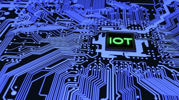
The Importance of PCB Design for IoT Devices:
IoT devices operate in diverse environments, demanding compactness, power efficiency, and robust connectivity. PCB designs specifically optimized for IoT applications are essential to meet these requirements. With our PCB design and layout services, we understand the unique challenges of IoT devices and strive to deliver solutions that enable seamless integration and exceptional performance.
Tailored Solutions for IoT:
At our PCB design company, we boast a team of experienced engineers who excel in creating high-quality, custom PCB designs for IoT devices. We understand that each IoT application has its own set of demands, ranging from complex multilayer layouts to high-speed signal integrity, RF circuitry, and power management solutions. By leveraging the latest components and cutting-edge technologies, we create PCB designs that maximize the capabilities of IoT devices while adhering to industry standards.
Collaboration and Expertise:
We believe in close collaboration with our clients to ensure that their specific IoT device requirements are met. Our engineers work closely with you, taking the time to understand your project goals, constraints, and specifications. With this valuable insight, we translate your ideas into innovative PCB designs that not only meet your expectations but also surpass them. Our expertise in advanced design tools and methodologies allows us to streamline the development process, reducing time-to-market without compromising on quality.
Reliability and Durability:
IoT devices often operate in challenging environments, and reliability is of paramount importance. Our rigorous testing procedures ensure that our PCB designs are robust, durable, and capable of withstanding the demands of IoT environments. We take pride in delivering solutions that stand the test of time, providing our clients with confidence in the longevity and performance of their IoT devices.
Driving the Future with Intellisense Technology:
The future of IoT lies in intelligent connectivity and seamless communication. Intellisense technology, powered by artificial intelligence and sensor data, empowers devices to gather and interpret real-time information, making them smarter and more intuitive. Our PCB design services for IoT devices are designed to support this advancement by providing efficient, compact, and reliable circuitry. By leveraging our expertise in PCB designs, we help businesses transform their IoT ideas into reality, enabling them to thrive in the era of intellisense technology.
Conclusion:
As the Internet of Things continues to revolutionize industries, the significance of PCB design services for IoT devices cannot be overstated. With our PCB design and layout services, we offer tailored solutions that meet the unique requirements of IoT applications. By partnering with our experienced engineers, you can unlock the potential of your IoT devices, ensuring seamless integration, optimal functionality, and a competitive edge in the ever-evolving IoT landscape. Embrace the power of PCB design and let your IoT devices thrive in the era of intellisense technology.
[…] Introduction:In the ever-expanding world of the Internet of Things (IoT), Printed Circuit Board (PCB) design services serve as the foundation for seamless […]